The design of the "Devious Digital Device" for Midnight Sun CTF 2019
After last year’s success, Calle asked me to again make a low-level logic circuit challenge for this year’s Midnight Sun CTF, and so this post will cover the “Devious Digital Device” challenge featured in Midnight Sun CTF 2019. I’ll start with a description of the board and how to solve the challenge, and then step back and walk through the design and development process.
All the code and schematics are available on GitHub.
Table of contents
The challenge
The instructions for the “Devious Digital Device” challenge were simple:
Category: Reversing
Our operatives have found this device inside the base. Please help us figure out what it does.
Note: Physical challenge. Go to the admin room to find the challenge.
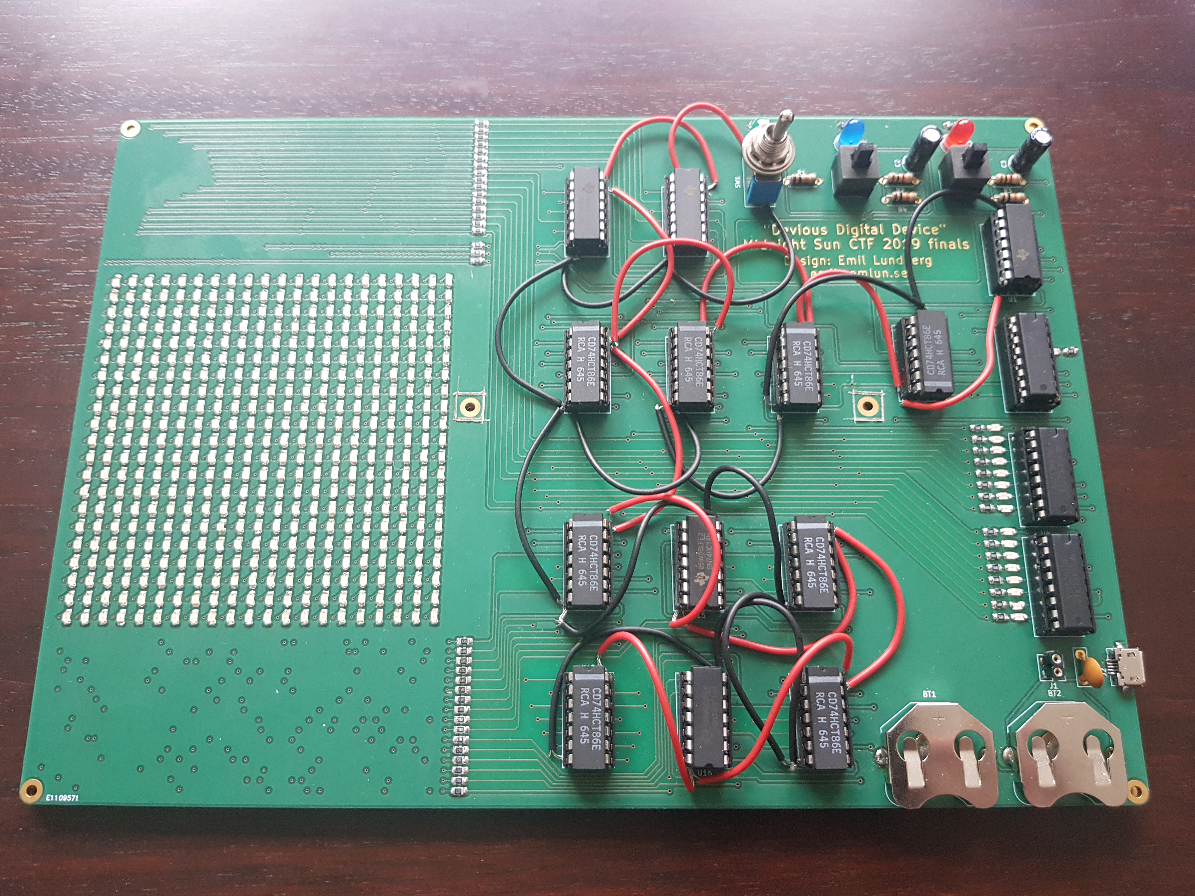
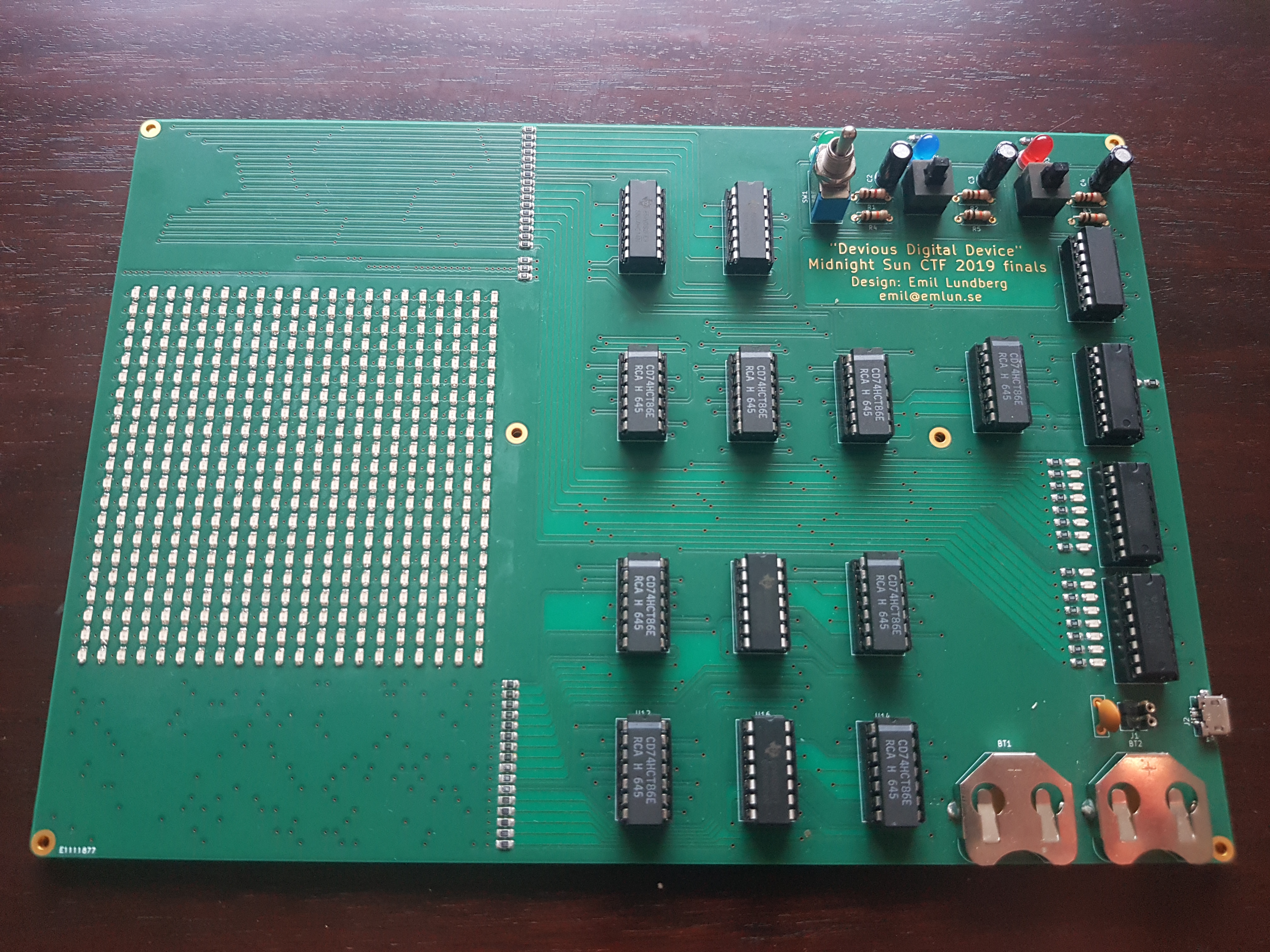
In the admin room, the contestants found four copies of the board shown in figure 1:

No further information was given - no hint of what the goal of the challenge is, no instructions on how to operate the board, etc. When operated, the board behaves as shown in figure 2:
From here, the intended path to a solution was something like this:
- Try pushing the buttons.
- Notice that the left button makes the lights move.
- See that the lights on the left seem to flash on and off somewhat randomly.
- Notice that the lights on the right “move” downwards when the left button is pushed.
- Identify the rightmost ICs, from the labels printed on them, as shift registers, and the lights on the right as the state of 2 of them.
- Notice that there seem to be some patterns in the lights on the left, that resemble parts of a QR code.
- Flip the board over and notice that there are visible tracks leading to three of the corners, but no visible tracks leading to the rest of the LEDs.
- Realize that those three corners make fixed patterns in a QR code.
- Ask yourself “under what circumstances do the corners make valid QR code corners?”
- Trace the visible tracks backward and conclude that their signals are a scrambled version of the shift register state, transformed by the 5 top-left ICs.
- Identify the scrambling ICs as NOT and XOR gates.
- Trace the tracks from end to end and form a Boolean equation system relating each LED signal to the 16 bits of the shift register state.
- Assume that the LED side of the equation system is supposed to make up the fixed corners of a QR code.
- Solve the equation system for the state that needs to be put in the shift registers.
- Trace the tracks from the flip switch and conclude that it inverts the input to the 2 shift registers holding the state.
- Reset the board, advance the state 16 steps and note down the resulting “default” shift register state.
- Reset the board and advance the state 16 steps, turning the flip switch on for the bits that differ between the noted “default” state and the equation solution from step 16.
- The board now shows a valid QR code, which yields the flag when decoded.
Some parts of this intended solution path were emergent consequences of the design, like the fact that you don’t actually have to deduce how the shift register inputs are generated. Other parts were more deliberate and guided the design of the board, like the end goal of reaching a valid QR code, how not all tracks are visible, and how only NOT and XOR gates were used to generate the scrambled LED signals.
Now let’s go back to the beginning and work through the design and development phases.
Phase 1: Ideation
Last year’s board was a stateless circuit, so this time we wanted to try doing a stateful one so that order of operations becomes significant. Calle suggested early on that we could use shift registers for this. This is an appealing idea: shift registers are cheap but nontrivial memory devices, but their function is still easy to understand even if you’ve never heard of them before. As described by Wikipedia:
[…] a circuit that shifts by one position the “bit array” stored in it, “shifting in” the data present at its input and ‘shifting out’ the last bit in the array, at each transition of the clock input.
We discussed some ideas like modeling a finite state machine and what could be done with that. The idea of significant order of operations reminded me of rotary combination locks, as prominently featured in old Jönssonligan films.

Still, we wanted a way to make the circuit a little interesting. Maybe draw the solution as some kind of pattern or image using LEDs?
That’s where we hatched the idea of drawing a QR code on an LED matrix, which I found really appealing. QR codes have some fixed patterns, which we can use as a ground truth for the solver to discover and use to solve the puzzle. So the flag would be encoded in the QR code and the challenge would be to first notice that the matrix is supposed to display a QR code, and then to figure out what combination of inputs make the fixed parts of the QR code valid. This was enough of a concept to start experimenting and prototyping.
Phase 2: Experimentation
With this rough concept in place I started working on how to realise the idea as a circuit. Most importantly I needed to decide how the LED matrix would work. The naïve way to implement an LED matrix is of course to just connect one wire to each LED so you can control them all independently. The problem is that this doesn’t scale very well, since you’d need N2 wires for an N by N grid. A common way to solve this is to instead power only one row of LEDs at a time, in which case you need only 2N wires for an N by N grid. The drawback of this approach, though, is that you need a high-frequency clock circuit to sweep through the rows fast enough to make them appear steadily lit. We want the circuit to be rather easy to reverse-engineer, so we didn’t want to add that kind of complexity even if it’s not hard to do.
I thought for a bit that I’d found a way to do something similar without needing the row-sweep, by connecting each row of LEDs’ power pins to one shift register output and each column’s ground pins to another shift register output. This turns out to work for a single LED, but not for a 2x2 grid. If you look closely in Figure 4 you can see there is no way to equate the Boolean equation to 1, since at least one of r0, r1, c0 or c1 would need to equal both 0 and 1 simultaneously.
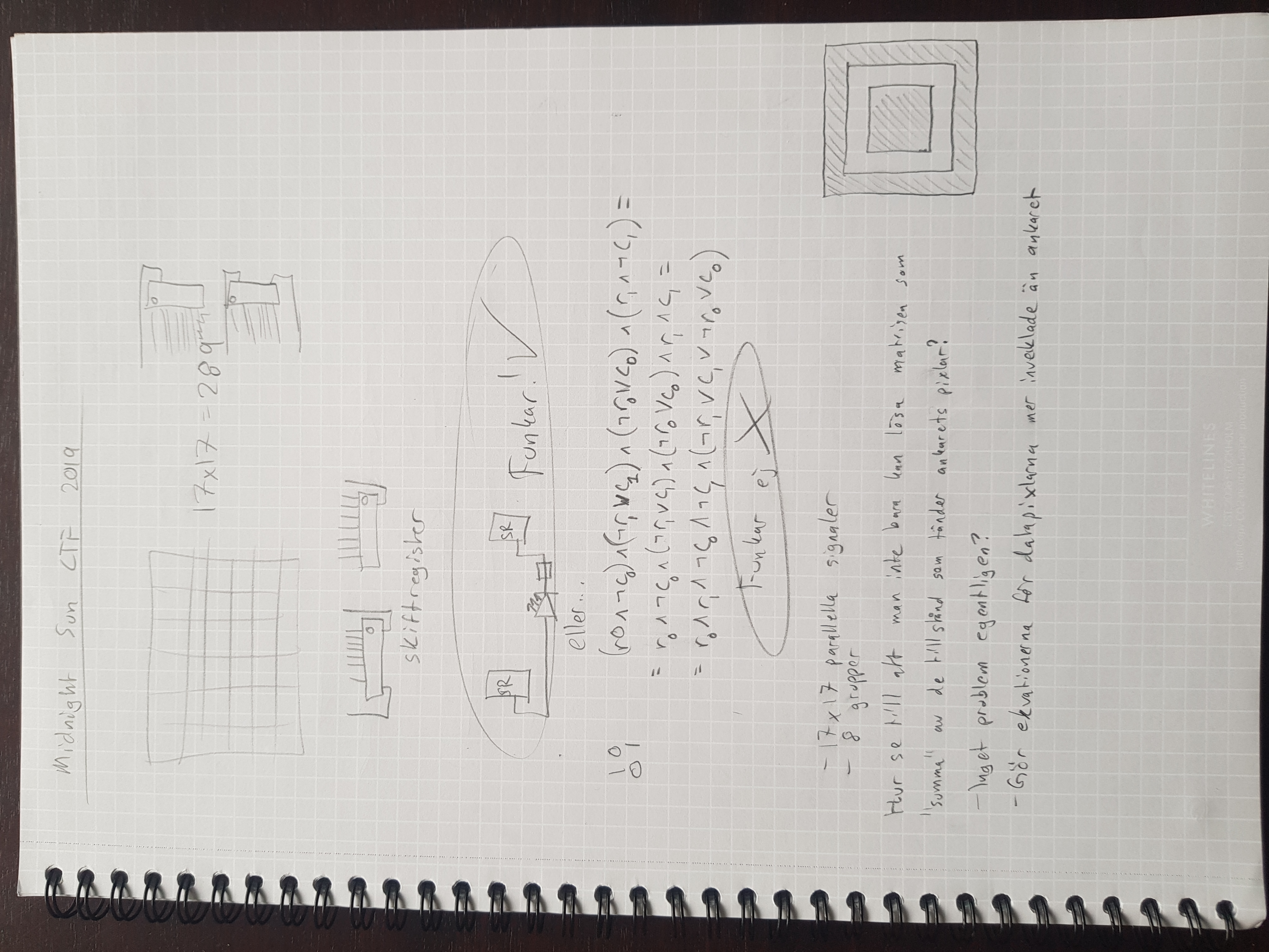
So that meant I was going to need N2 parallel wires after all. Next, then, was to choose the QR code type. In addition to multiple sizes of standard QR codes, the smallest of which is 21x21 pixels, there is also a Micro QR variant that goes down to 17x17 pixels. Unfortunately none of the easily available QR code readers I tried seemed to support this format, which meant I’d need to use a standard 21x21 QR code and no less than 441 LEDs.
Generating and simulating the LED matrix
As mentioned previously, I wanted the contestants to discover on their own that it seems like the LED matrix is supposed to show a QR code in the end, so my next step was to simulate what the LED matrix could look like as you operate the board. I wrote an Octave/MATLAB script to visualise this and try out some ways it could work. Starting with the solution state:
M = 1;
_ = 0;
qr_code = [
    M M M M M M M _ M _ _ _ _ _ M M M M M M M
    M _ _ _ _ _ M _ M M _ _ M _ M _ _ _ _ _ M
    M _ M M M _ M _ M _ M _ _ _ M _ M M M _ M
    M _ M M M _ M _ M _ _ M M _ M _ M M M _ M
    M _ M M M _ M _ _ M M M _ _ M _ M M M _ M
    M _ _ _ _ _ M _ M M _ M M _ M _ _ _ _ _ M
    M M M M M M M _ M _ M _ M _ M M M M M M M
    _ _ _ _ _ _ _ _ _ M M M _ _ _ _ _ _ _ _ _
    M M _ _ M M M _ _ _ _ M M _ _ M _ M M M M
    M _ _ _ _ M _ _ _ M M M _ _ M M M _ _ M _
    M M M M M _ M M _ _ M _ _ _ _ _ M _ _ M _
    M _ _ M _ M _ M M M _ M M M _ M M _ _ M _
    M _ M M _ M M _ _ M _ M M _ _ _ M _ _ _ _
    _ _ _ _ _ _ _ _ M _ M _ _ M _ _ M M M M _
    M M M M M M M _ _ M M _ _ M M _ M M _ M _
    M _ _ _ _ _ M _ M _ M _ _ M _ _ _ _ _ M _
    M _ M M M _ M _ M M _ _ M _ _ M _ _ _ M M
    M _ M M M _ M _ _ M M M _ M M _ M M _ _ M
    M _ M M M _ M _ _ M M M _ M M _ M M M _ _
    M _ _ _ _ _ M _ M M _ M _ M _ _ M _ _ _ _
    M M M M M M M _ M _ _ _ _ M _ _ M _ _ _ M
];
I divided the cells of this matrix into 35 groups:
- The three distinct “anchor frames”:
a1,a2,a3 - The 16 white pixels in the anchor:
b1,b2, …,b16 - 8 groups of black data pixels:
o1,o2, …,o8(ofor “ones”) - 8 groups of white data pixels:
z1,z2, …,z8(zfor “zeroes”)
and laid these out in accordance with the qr_code solution:
m = [
  a1 a1  a1  a1  a1  a1  a1 z1 o1 z2 z3 z4 z5 z6 a2 a2  a2  a2  a2  a2 a2
  a1 b1  b2  b3  b4  b5  a1 z7 o2 o3 z8 z1 o4 z2 a2 b13 b14 b15 b16 b1 a2
  a1 b16 a1  a1  a1  b6  a1 z3 o5 z4 o6 z5 z6 z7 a2 b12 a2  a2  a2  b2 a2
  a1 b15 a1  a1  a1  b7  a1 z8 o7 z1 z2 o8 o1 z3 a2 b11 a2  a2  a2  b3 a2
  a1 b14 a1  a1  a1  b8  a1 z4 z5 o2 o3 o4 z6 z7 a2 b10 a2  a2  a2  b4 a2
  a1 b13 b12 b11 b10 b9  a1 z8 o5 o6 z1 o7 o8 z2 a2 b9  b8  b7  b6  b5 a2
  a1 a1  a1  a1  a1  a1  a1 z3 o1 z4 o2 z5 o3 z6 a2 a2  a2  a2  a2  a2 a2
  z7 z8  z1  z2  z3  z4  z5 z6 z7 o4 o5 o6 z8 z1 z2 z3  z4  z5  z6  z7 z8
  o7 o8  z1  z2  o1  o2  o3 z3 z4 z5 z6 o4 o5 z7 z8 o6  z1  o7  o8  o1 o2
  o3 z2  z3  z4  z5  o4  z6 z7 z8 o5 o6 o7 z1 z2 o8 o1  o2  z3  z4  o3 z5
  o4 o5  o6  o7  o8  z6  o1 o2 z7 z8 o3 z1 z2 z3 z4 z5  o4  z6  z7  o5 z8
  o6 z1  z2  o7  z3  o8  z4 o1 o2 o3 z5 o4 o5 o6 z6 o7  o8  z7  z8  o1 z1
  o2 z2  o3  o4  z3  o5  o6 z4 z5 o7 z6 o8 o1 z7 z8 z1  o2  z2  z3  z4 z5
  z6 z7  z8  z1  z2  z3  z4 z5 o3 z6 o4 z7 z8 o5 z1 z2  o6  o7  o8  o1 z3
  a3 a3  a3  a3  a3  a3  a3 z4 z5 o2 o3 z6 z7 o4 o5 z8  o6  o7  z1  o8 z2
  a3 b5  b6  b7  b8  b9  a3 z3 o1 z4 o2 z5 z6 o3 z7 z8  z1  z2  z3  o4 z4
  a3 b4  a3  a3  a3  b10 a3 z5 o5 o6 z6 z7 o7 z8 z1 o8  z2  z3  z4  o1 o2
  a3 b3  a3  a3  a3  b11 a3 z5 z6 o3 o4 o5 z7 o6 o7 z8  o8  o1  z1  z2 o2
  a3 b2  a3  a3  a3  b12 a3 z3 z4 o3 o4 o5 z5 o6 o7 z6  o8  o1  o2  z7 z8
  a3 b1  b16 b15 b14 b13 a3 z1 o3 o4 z2 o5 z3 o6 z4 z5  o7  z6  z7  z8 z1
  a3 a3  a3  a3  a3  a3  a3 z2 o8 z3 z4 z5 z6 o1 z7 z8  o2  z1  z2  z3 o3
];
I chose this arrangement of the a and b groups so that those corners would
stand out a little bit while not making it too blatantly obvious. The frames of
the corners can flash on and off independently and are quite conspicuous, but
their shape is not immediately obvious since the b pixels of the internal
“rings” will rarely be off all at once. The b rings are also rotated 90°
relative to each other to lightly disguise the fact that they’re all identical.
Meanwhile, the data pixels don’t have any visible pattern to them, so they’re just arbitrarily distributed into groups one by one in a repeating pattern. This way, each group is spread out so that changes to the state cause changes all over the matrix.
Finally, I needed to to come up with a suitable way to generate these 35 signals
from one 16-bit state x. I generated a random solution with 8 bits of 1 and 8
bits of 0:
% solution = randperm(16) >= 9
solution = [1 1 0 1 0 0 0 1 0 0 1 1 1 0 0 1]';
h = x(solution == 1);
l = x(solution == 0);
You can also see that I’ve let h (“high”) and l (“low”) represent the bits
of the state x where the solution has 1s and 0s, respectively. How x is
generated is covered in the next section.
With this I could let the 16 b signals correspond directly to bits of the
state x, with the hs inverted since the solution has all the b pixels
turned off:
b = [~h; l];
The a signals could simply be XORs of an odd number of hs and any number of
ls, since the solution has all the a pixels turned on:
a1 = xor(h(1), h(2), h(3), l(1), l(2), l(3));
a2 = xor(h(4), h(5), h(6), l(4), l(5));
a3 = ~xor(h(7), h(8), l(6), l(7), l(8));
Finally, each of the os could be the XOR of one random h and one
random l, and each of the zs could be the inverted XOR of one random h and
one random l.
z_indices = [
  % [ randperm(8, 2); ... ]
  2   6
  8   5
  5   4
  7   5
  6   5
  3   1
  1   8
  7   4
];
o_indices = % (generated in the same way)

z = ~xor(l(z_indices(:, 1)), h(z_indices(:, 2)));
o = xor(l(o_indices(:, 1)), h(o_indices(:, 2)));
All of the above code is available on GitHub.
With all this in place I could simulate how the LED matrix could look while being fed some random sequence of inputs, shown in figure 5:
If we instead modify the state by flipping one bit at a time, we get the behaviour shown in figure 6:
Here we can see that even flipping a single bit of the state always makes some
noticeable change to the LED matrix. This is one of the effects I was going for,
and the main reason why I chose to use mostly XORs to scramble the state - since
an XOR of any number of inputs always flips its output if you flip one (or any
odd number) of the inputs. Likewise, you can see that each bit flip also flips
exactly one of the three a corners, since these three signals are made from
non-overlapping XORs that together cover all bits of the state.
All in all, this achieves an effect of looking consistently chaotic at first glance, while still hinting pretty firmly at the QR patterns if you’re a little observant. That’s exactly the effect I was going for, so I was quite happy with these results.
Next, I needed a way to generate that input signal x that all this builds on.
This is the role of the shift register state machine.
Designing the state machine
With a good idea of how to draw the LED matrix, the next step was to design the state machine that would generate the input signal from which to generate the matrix. For this I figured I could use some shift registers feeding back into themselves through some Boolean gates. Taking the serial output from that should hopefully result in some suitably complicated bit sequence.
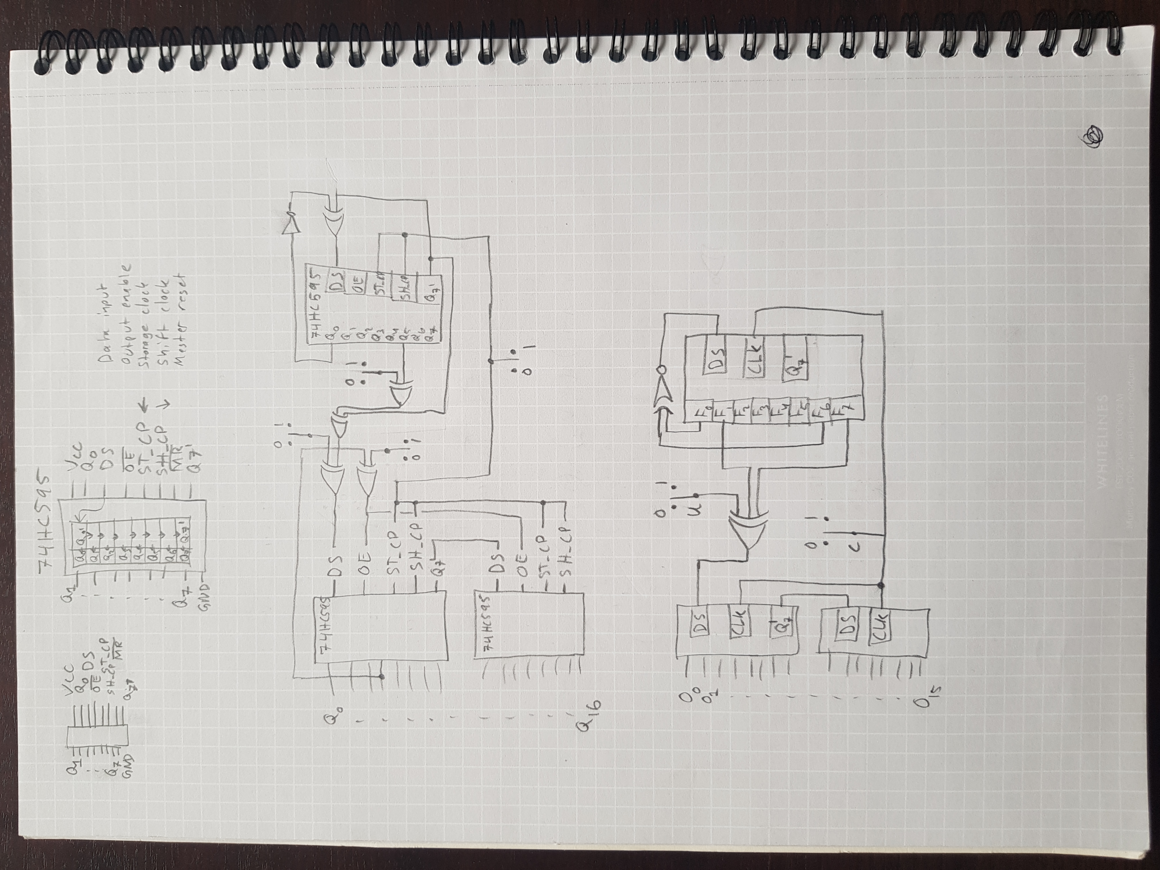
Without thinking too much about it I sketched out a possible structure, shown in the middle of figure 7. Note how the rightmost shift register feeds back into itself and how there are two manual switches for manipulating the data being fed into the leftmost shift registers. The second sketch, shown at the bottom, has a significantly simplified connection structure, since stacking multiple XOR gates doesn’t really do anything. The second user input switch also doesn’t really do anything since one can be completely ignored without losing any control of the signal.
Note also the inverters on the feedback input, at the top-right of each sketch. These are necessary so that the state register doesn’t get stuck if it happens to be filled with all zeroes - which happens when a reset signal is sent, for example.
Again I used Octave to simulate some possible configurations, trying different ways to connect the feedback loop and how to mix in user input. Figure 8 shows a simulation of the bottom configuration in figure 7, with data flowing from right to left like in the sketch:
Figure 8: Simulation of the state machine with occasional user input. DSF is the serial input to the rightmost shift register, F’ is its internal storage register and F is its output registers. u is the user input switch. DSO, O’ and O are the serial input, internal storage register and output registers of the two leftmost shift registers.
As you can see, this produces a somewhat complicated bit sequence. It’s not random by any stretch, but it just needs to be some nontrivial pattern, so it’s all good. In fact, it’s a bit sneaky because it looks like a simple pattern at first but then reveals more complexity as time goes on. This seemed to work well enough, so the bottom sketch in figure 7 actually ended up being used in the final circuit.
With that, most of the design uncertainties had been settled, and it was time to move on to designing the actual circuit board.
Phase 3: PCB design
I covered most of what goes into CADing a circuit last time, and this one isn’t much different. The Boolean functions for the state scrambler, explained above and summarised in figure 9, are straightforward to implement with NOT and XOR gates, and the rest is mostly connecting the dots between the components.
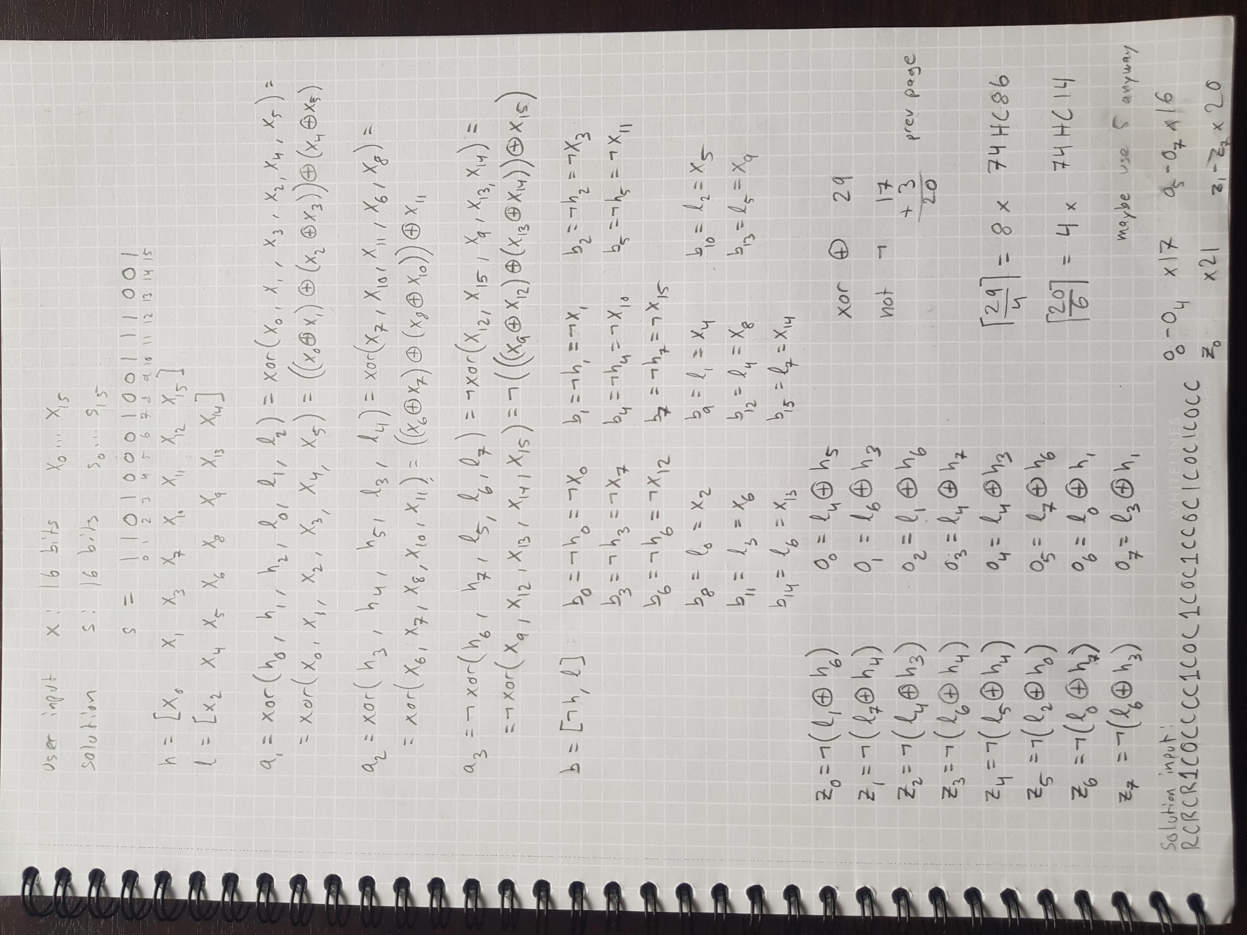
Figure 10 shows the main circuit schematic. At the far left are the power connectors and the input switches: a flip switch for the user input signal, a push button to pulse the shift register clock signals, and a push button to send a reset pulse to the shift registers. These switches’ states are indicated by a green, blue and red LED, respectively, although the colours aren’t documented in the schematic. Proceeding to the right we see the shift registers, the state feedback loop and the state LEDs, and then the state scrambler. Here you can see how the equations in figure 9 are encoded as wires (h2 = x3) and logic gates (o2 = l1 ⊕ h6). Finally, the scrambled signals are fed into the LED matrix subassembly shown in figure 11.

Figure 10: The circuit schematic. The component labeled
led-matrix.sch is a subassembly, shown in figure 11.

The least straightforward bit of this was to debounce the switches, because I don’t actually know how to do that properly. We had a previous version manufactured where the input switch wasn’t debounced since it’s a toggle switch and not a push button, and that ended up interfering with the two push buttons, sometimes triggering a reset signal when flipped. Luckily, this never happened in the second and final version of the board which has all three switches debounced.
Laying out the PCB schematic was time-consuming - dominated by routing tracks - but also straightforward. With the circuit schematic in place, KiCAD keeps track of what needs to connect where, so all you need to do is lay out the component footprints and wire them up without crossing the wires - which KiCAD will helpfully prevent you from doing.
I chose to use SMD components for the matrix and state LEDs and their resistors to keep them compact, and through-hole components for everything else because they’re easy to work with. We decided to make this a 4-layer board so we could hide the connections to the data pixels, because otherwise it would be possible to correlate the data pixels with the (assumed) known fixed pixels and solve the matrix without needing to actually enter the correct state. The 2 extra layers also happened to make it possible to route all 441 tracks to the LED matrix - as you can see in figure 12, I had to get a little creative to fit them even on 4 layers. It might not have been possible with only two layers.


You can also see how the corner pixel wires come in from the top while the data pixel wires come in from the bottom, and that the scrambling ICs are divided into one group above and one below the wide band of tracks down the middle of the front layer. This was done to hint that the bottom group of ICs is for generating the hidden connections, so you can concentrate on decoding the connections for the top group.
I’ll also note one more thing for any budding PCB designers out there: I’ve found that routing tracks becomes much easier if you try to stick to one direction per layer. For example, you can see in figure 12 that most tracks on the front layer run horizontally while most tracks on the back layer run vertically. This makes it much less of a headache to avoid running them into each other, though I guess it might increase the number of vias needed.
Digression aside, that concludes the design of this circuit board. Once the boards and components are delivered, assembly is again time-consuming but straightforward. In the end the circuit worked well - except powering it with batteries didn’t work as well as I thought; apparently I don’t understand battery physics - and the contestants liked the challenge, so I’m quite pleased with the result. Of course, all of the schematics are available on GitHub.
Thank you for reading, and good luck and have fun with your own circuit designs! If you’d like to contact me with any comments or questions of any kind, feel free to e-mail me or ask Calle.
Bloopers and funsies
There’s always some mistakes to be made and some fun to be had, so here are a few other pictures that didn’t fit into the main design walkthrough.

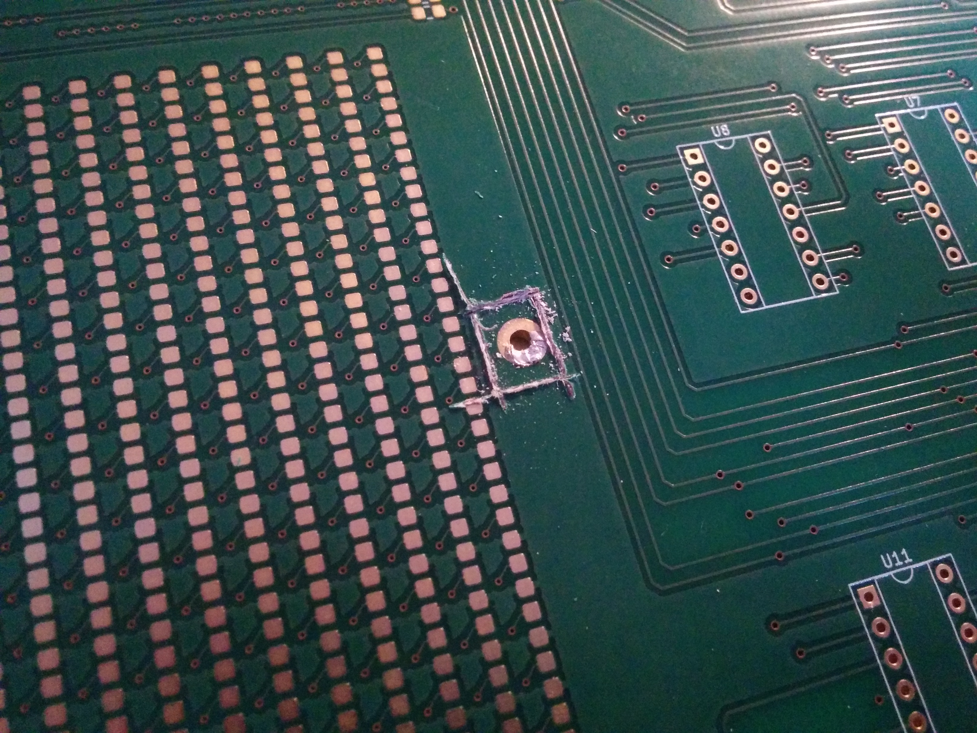
The first version of the board had 2 design mistakes. The first was that I accidentally short-circuited the VCC and GND zones, because I forgot to recompute the zones after adding two mounting holes. So I had to do some precision surgery on the prototype board to disconnect the mounting holes - that is, stab it with a Mora knife until it worked.